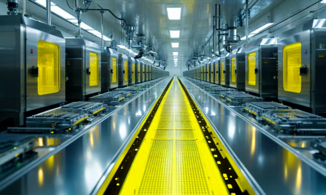
One of the most persistent myths in the quantum computing industry is that making quantum hardware is fundamentally different from making classical chips. The reality, at least for germanium spin qubits, is far more encouraging: the fabrication of our quantum processors uses tools, materials, and techniques already established in semiconductor manufacturing facilities around the world.
This is not a minor footnote. It is arguably the defining commercial advantage of the germanium qubit platform — the reason why scale-up is an engineering challenge rather than a physics moonshot.
The Quantum Dot: A Transistor's Cousin
A germanium spin qubit is defined by a quantum dot — a nanoscale region of semiconductor material where individual holes (the absence of electrons in the valence band) can be trapped and controlled. At first glance, this sounds exotic. But the physical structure of a quantum dot device looks remarkably like a transistor: gate electrodes patterned on top of a semiconductor heterostructure, separated by thin dielectric layers, with source and drain contacts on either side.
The key difference is scale and precision. Transistors in modern processors are measured in nanometers, and so are quantum dots. But where a transistor is designed to be a reliable switch that works for billions of cycles, a quantum dot must be designed to confine exactly one hole with sufficient isolation from its environment to maintain quantum coherence. This requires tighter control over material interfaces, lower defect densities, and more precise gate voltage control — but it does not require fundamentally different manufacturing equipment.
Epitaxial Germanium: Grown on Silicon Wafers
The quantum well at the heart of our devices is a strained germanium layer, grown epitaxially on a silicon or silicon-germanium buffer on a standard 300mm silicon wafer. Epitaxial growth of germanium on silicon is a mature technique used in high-performance RF transistors and photonic devices. The equipment — chemical vapor deposition (CVD) reactors — is available at most major semiconductor research institutes and foundries.
The germanium quantum well is typically 10-20 nm thick, sandwiched between silicon-germanium barrier layers that provide both quantum confinement and strain engineering. The strain in the germanium layer is critical: it modifies the band structure in a way that enhances hole mobility and, crucially, reduces the complexity of the spin-orbit coupling tensor, making qubit control more straightforward.
Gate Patterning: Standard Lithography, Extreme Precision
The gate electrode stack above the quantum well is patterned using electron-beam lithography (EBL) at the research stage and compatible with deep-UV lithography for production. Gate pitches in our current devices are in the range of 30-50 nm — within the capabilities of advanced-node lithography tools already deployed at major foundries.
The gate stack itself uses industry-standard materials: aluminum oxide or hafnium oxide as gate dielectrics (the same high-k dielectrics used in modern FinFETs), and aluminum or titanium nitride as gate metals. No exotic superconductors, no laser-cooled atoms, no fiber optic connections into a cryostat. Just the standard palette of semiconductor manufacturing materials, applied with exceptional care to interface quality and contamination control.
Cryo-CMOS Integration: The Control Electronics Challenge
Fabricating the qubit chip is only half the manufacturing challenge. The other half is the control electronics. Each qubit requires multiple gate voltage signals for initialization, single-qubit rotations, two-qubit interactions, and readout. At the scale of hundreds or thousands of qubits, routing all those signals from room-temperature electronics down to a millikelvin cryostat is physically impossible — the heat load from the cables alone would overwhelm the cooling power of the dilution refrigerator.
The solution is cryo-CMOS: classical CMOS circuits designed to operate at temperatures of 4 Kelvin or below, located close to the qubit chip inside the cryostat. Because germanium spin qubits use electrical gate signals rather than microwave pulses, the cryo-CMOS control chips can be relatively simple digital-to-analog converters and signal routing switches — exactly the kind of circuits that CMOS logic handles efficiently.
Several semiconductor companies and research groups have already demonstrated cryo-CMOS multiplexers and readout circuits operating at 4K. Integration of qubit chips with cryo-CMOS control chips, either by flip-chip bonding or 3D integration, is a clear and achievable engineering roadmap — not a speculative future capability.
Why Foundry Compatibility Changes Everything
The practical implication of all this is profound. When Groove Quantum reaches the scale where fabricating devices in-house is no longer efficient, we can in principle transfer our process to an established semiconductor foundry. The transition from research prototypes to manufactured products does not require building a custom fab from scratch — it requires process transfer to an existing one.
This dramatically de-risks the commercialization path. The capital investment required to scale production of germanium qubit processors is far lower than the equivalent investment for qubit technologies that require genuinely bespoke manufacturing — and the timeline to scaled production is correspondingly shorter. For investors and industry partners evaluating quantum hardware companies, this is not a trivial consideration.
Quantum computing's commercial future will be built in semiconductor fabs. Groove Quantum is building hardware that those fabs can make.